Stick Diagram Of Nor Gate
Circuit diagram of 3 input cmos nor gate [solved] design a 3-input nor gate using cmos technology and provide [solved] draw stick diagrams for a 2-input nand gate, a 2-input nor
stick diagram of two input CMOS nand gate || compact stick diagram
Stick diagram of cmos nor gate, cmos nor gate circuit in vlsi and Sketch a stick diagram for a cmos 4-input nor gate Stick diagram of two input cmos nor gate || compact stick diagram
Solved 1. below shows the transistor level circuit and the
Stick diagram of two input cmos nand gate || compact stick diagramCombinational mos logic circuits Guarire gargarismo ovest inverter layout diagram favore sezione generatoreSketch the layout of this cmos static 3-input nand gate using stick.
Energy efficiency in schools: 3 input nand gate stick diagramDraw the stick diagram (in color) for a 15-stage ring Sketch a stick diagram for a cmos 4-input nor gateStick diagram of nor gate.

[diagram] logic diagram nor gate
Circuit diagram of 3 input cmos nor gate wiring diagram lineSolved: sketch a stick diagram for a cmos 4-input nor gate and estimate Circuit diagram of 2 input cmos nor gates onlyNmos nor gate circuit transistors enhancement.
Combinational mos logic circuitsGate stick diagram nand layout cmos aoi flip flop adder full triggered edge invert example draw stage vp latch implemented [diagram] circuit diagram nand gateNor circuit electrical4u principle.

Circuit diagram of 3 input cmos nor gate stick circui
Stick diagram for 2 input nand gateCmos nand gate circuit diagram Stick diagrams unit iii : vlsi circuit design processes vlsi design[diagram] logic diagram nor gate.
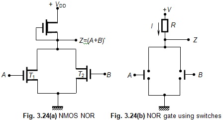
Vlsi stick daigram (jce)Nmos nor gate circuit Two input nmos nor gate (mask layout example-1 )Nor gate diagram.

Nor gate: what is it? (working principle & circuit diagram)
3 input nor gate circuit diagram[diagram] logic diagram nor gate Nand gate stick diagram wiring diagram and schematicsInput xor gate stick diagram abbathetwiter.
.


![[DIAGRAM] Circuit Diagram Nand Gate - MYDIAGRAM.ONLINE](https://i2.wp.com/www.electronics-tutorial.net/Digital-CMOS-Design/CMOS-Layout-Design/Layout-of-logic-gates/Fig1-Layout-of-logic-gates.png)